




fig8
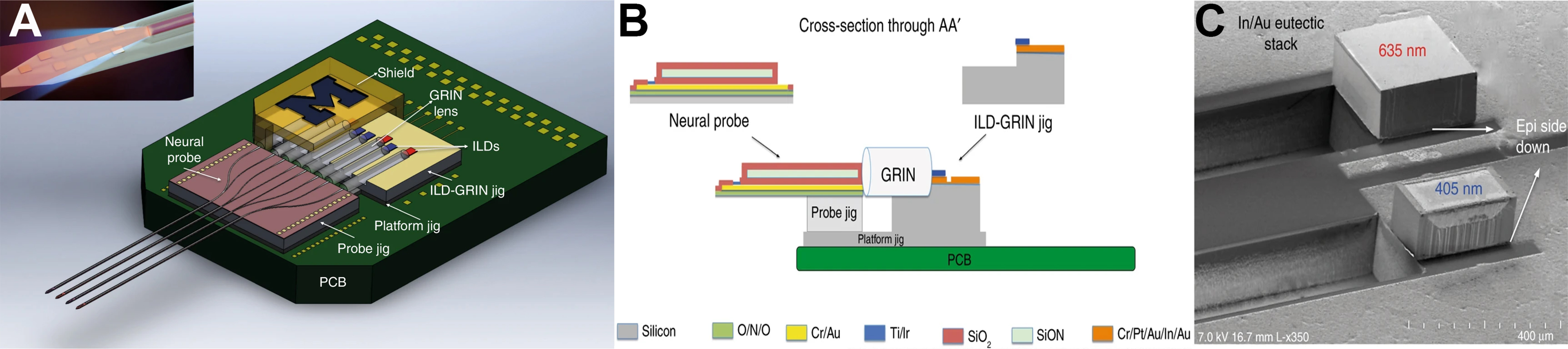
Figure 8. Schematic of multishank multicolor fiberless optoelectrode assembled on a printed circuit board[97]: (A) Device fabrication details; the inset is the local enlargement of the tip of the probe; (B) Fabricated neural probe shank tips with monolithically integrated dielectric waveguides; (C) High-magnification SEM image of epi-side down flip-chipped 405 and 635 nm ILDs on the ILD-GRIN. This figure is adapted from Ref.[97]. Copyright © 2018 The Author(s). SEM: Scanning electron microscopy; ILDs: injection laser diodes; GRIN: gradient-index; PCB: printed circuit board.