




fig6
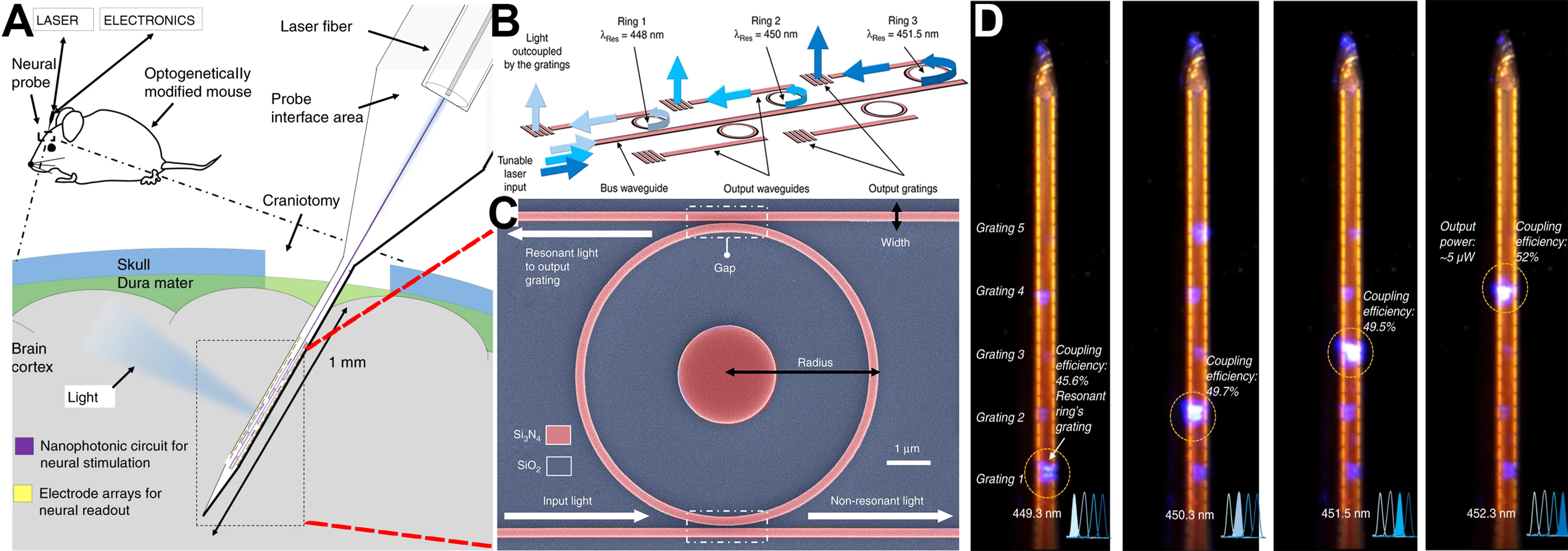
Figure 6. Small footprint and passive optoelectrode for electrophysiology and optogenetic applications[93]: (A) Schematic illustration of the neural probe; (B) Schematic illustration of the nanophotonic circuit in the probe tip area; (C) SEM image of a SiN ring resonator; (D) Optical microscope image of the tip of the assembled neural probe. This figure is adapted from Ref.[93]. Copyright © 2021 The Author(s). SEM: Scanning electron microscopy.