




fig12
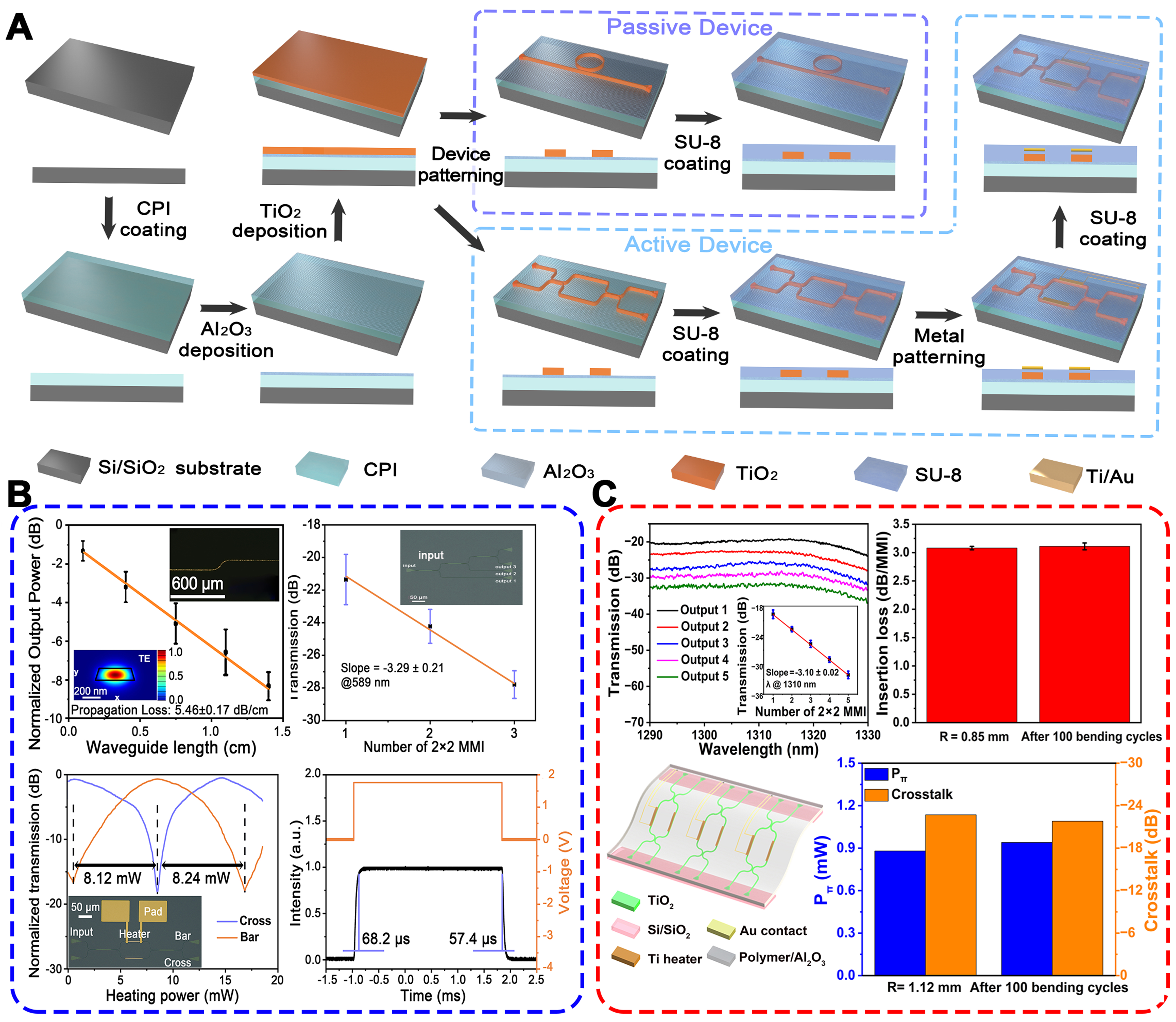
Figure 12. TiO2 integrated photonic monolithic integration process on flexible substrate[48]: (A) Schematic diagram of the device fabrication process. (B) TiO2 waveguide integrated devices at 589 nm: upper left: propagation loss; upper right: the insertion loss of 2 × 2 MMI; bottom left: the power of TOS; bottom right: the response time of TOS. (A and B) are reprinted with permission from Ref.[48], Copyright © 2025 Optica Publishing Group. (C) Flexible TiO2 waveguide integrated devices at 1,310 nm[57]: upper: Flexible 2 × 2 MMI measurement; bottom: Flexible TOS measurement. (C) is reprinted with permission from Ref.[57], Copyright © 2023 Optica Publishing Group. MMI: Multimode interference; TOS: thermo-optic switch; CPI: colorless polyimide; TE: transverse electric.