fig3
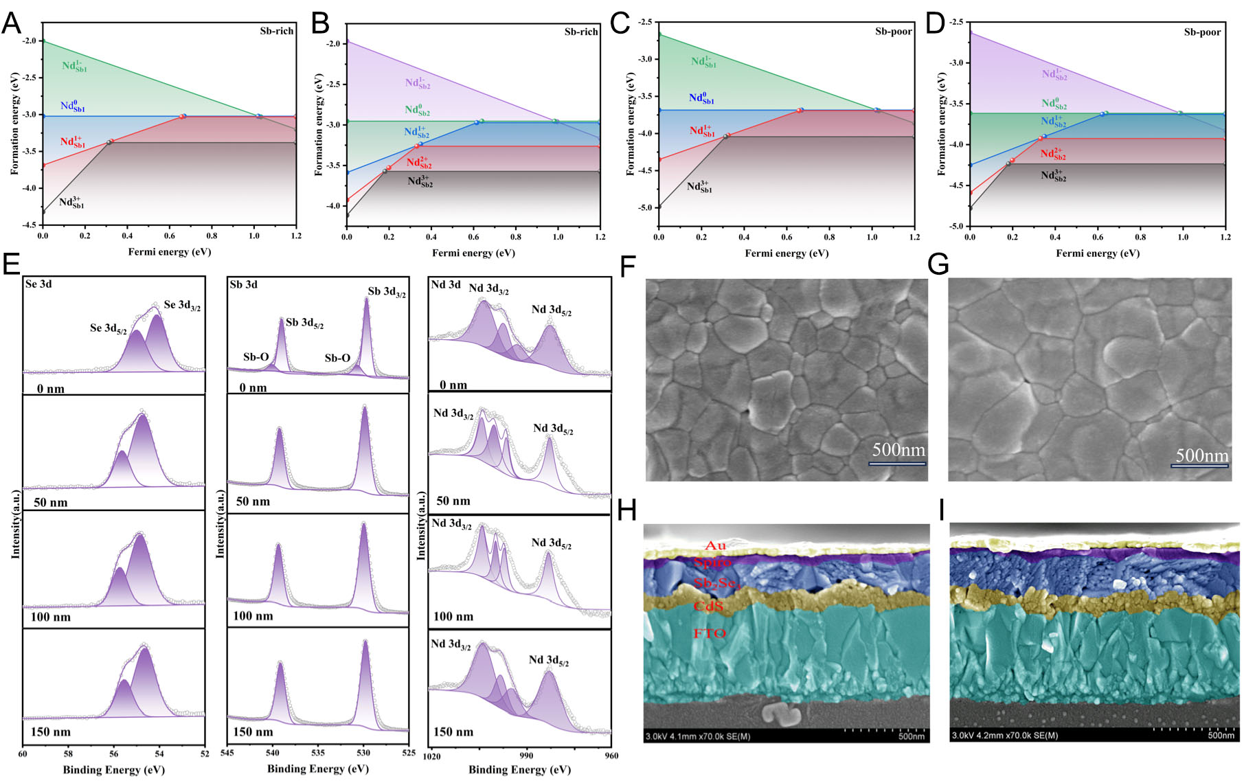
Figure 3. (A-D) Relationship between point defects and the Fermi level in Nd-doped Sb2Se3 thin films under different chemical potential conditions (Sb-rich and Sb-poor), (E) Variation in Se/Sb/Nd contents in Sb2Se3 samples at different etching depths, (F and G) Surface morphology of Sb2Se3 films with W Nd-CdS and W/O Nd-CdS, (H and I) Cross-sectional images of Sb2Se3 films with W Nd-CdS and W/O Nd-CdS.